Simulation overview
The Simulink work was a design-time aid — it informed the topology, modulation, and gate-drive choices before any silicon was committed. It was not a live model and is not part of the runtime control loop.
Headline results
| Metric | Value | Source |
|---|---|---|
| Predicted THD (pre-filter, LS-PWM) | 4.9 % | LS-PWM model output, validated against the IEEE 519-2022 < 8 % limit |
| Predicted efficiency | > 95 % | Pre-filter, ideal switches, design-target load (≈ 400 W) |
| Predicted gate-drive failure mode | IR2110 floating reference | The simulation that killed the IR2110 path and forced the TLP250 choice |
What was simulated
Three Simulink models are kept in simulation/simulink/:
| Model | What it covers |
|---|---|
chb-5level-v1.slx |
First-pass 5-level CHB with IPD LS-PWM, ideal switches, resistive load. The model that produced the 4.9 % THD figure. |
chb-5level-v2.slx |
Revised topology with the gate-drive sweep (IR2110 vs. TLP250) added. The IR2110 path is where the floating-reference failure showed up. |
chb-5level-rl-nospike.slx |
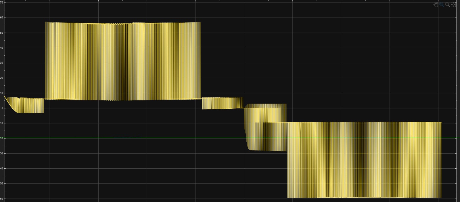
LC-filtered variant with an RL load — used to characterize the wavy-current artefact and tune the snubber. |
What the model does not capture
- Parasitic inductance. Gate-loop and DC-bus parasitics that cause real-world voltage spikes are not in the ideal-switch model. The snubber design (22 Ω 2 W + 2.2 nF / 630 V) was specified to bound these on the bench, not in simulation.
- Dead time. Simulink uses ideal complementary switches; the firmware enforces 3 µs dead time on the IRFB4110. Shoot-through margin is verified on the scope, not in the model.
- Sensor noise + isolation. The MCP3201 + 6N137 chain has SPI line inversion and rail-stuck detection in the firmware; none of that is reflected in the simulation's idealized sensor model.
- Thermal coupling. The model assumes both bridges at room temperature; the bench validation actually measured per-bridge MOSFET case temperatures.
The bench-validated numbers are what go into the final report. The simulation explains the why of the topology and gate-drive choices.
See also
- THD analysis — the FFT side-by-side and the per-harmonic content.
- Model architecture — block-by-block walk-through.
- PSC vs. LSPWM design note — the cascade-balance argument that drove the switch from IPD to PSC after the simulation was complete.