Grounding fix
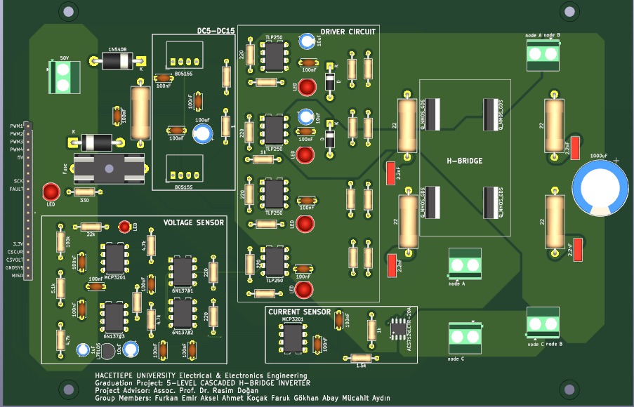
Single-sentence summary. Iteration 3 of the PCB had a parasitic coupling between 5V_GND (controller side) and 50V_GND (bridge side) that defeated the isolation architecture. Iteration 4 fixed it through stricter layer separation and via placement on the 4-layer JLCPCB stack-up. The populated boards now run clean — confirmed by the team.
The two grounds the project deliberately keeps separate
The CHB topology requires the controller side and each bridge side to be galvanically isolated (see CHB isolation). The board uses three distinct reference nets:
| Net | Where it lives | Reference |
|---|---|---|
| 5V_GND | STM32 Nucleo, USB / VCP, dashboard | System ground (USB shield-tied, ultimately mains-earth via the bench PC) |
| 50V_GND (lower bridge) | Bridge 1 power stage, its TLP250 outputs, its MCP3201 | Floats at the lower-bridge DC source's negative rail |
| 50V_GND (upper bridge) | Bridge 2 power stage, its TLP250 outputs, its MCP3201 + current MCP3201 | Floats at the upper-bridge DC source's negative rail (i.e. at Bridge 1's output node) |
These three nets are connected only through the isolation parts: TLP250 LED → photodetector, B0515S primary → secondary, 6N137 LED → photodetector. There is no copper trace, no via, no shared shield, no shared connector pin that bridges them on a correctly-designed board.
What went wrong in iteration 3
The team's iteration-3 layout had two coupling paths between 5V_GND and 50V_GND that should not have been there. The combined effect was measurable common-mode noise on the controller's GPIO pins whenever Bridge 2 was switching at the cascade peak — exactly the failure mode that CHB isolation is supposed to prevent.
The specific issues (reconstructed from the bench notes and the iteration-3 KiCad backup; the team can fill in details):
- Shared via stitching across the isolation boundary. A run of decoupling vias along the edge of the isolated island connected to the inner ground plane on layer 2 — which was a continuous 5V_GND pour. The intent was to give the isolated MCP3201 a clean decoupling return, but the via stitching effectively shorted the islands together at AC through the inner-layer pour.
- Insufficient creepage on the optocoupler footprints. The 6N137 and TLP250 footprints had the input-side and output-side copper too close — a few mil at the closest point. Under the cascade-peak common-mode swing (50–100 V), the parasitic capacitance across that gap coupled enough current to make the SPI reads marginal.
The result was the kind of intermittent fault that's hard to diagnose: the dashboard's STATUS would occasionally show garbage ADC values, the firmware's SENSOR_LOST debounce would trigger sporadically, and switching from sustained run to PRECHARGE could leave the controller in a confused state.
How iteration 4 fixed it
The fix was physical separation, not logical separation. Three changes:
1. 4-layer stack-up with dedicated, separated ground planes
Instead of a continuous inner ground plane, the iteration-4 stack-up uses two separate inner pours:
| Layer | Role |
|---|---|
| L1 (top, 1 oz) | Signal + power-stage traces. Routed in distinct regions for controller side vs. each bridge side, with no traces crossing the isolation boundary. |
| L2 (inner, 0.5 oz) | 5V_GND pour in the controller region only. No copper extends into the isolated bridge regions. |
| L3 (inner, 0.5 oz) | Per-bridge 50V_GND pours, each in its own bridge region. No connection between them or to 5V_GND. |
| L4 (bottom, 1 oz) | Same regional split as L1. Isolated SPI return runs through the bridge-region copper only. |
This is the master plan rule "stitched ground vias along the boundary between primary and isolated regions" — the via stitching is now within each region (binding L1↔L2 in the controller region, L1↔L3 in each bridge region) and never crosses the isolation boundary.
2. Increased creepage at every isolation crossing
The TLP250, 6N137, and B0515S footprints in iteration 4 have explicit keep-out regions between the input-side and output-side pads. The DIP-8 packages physically span the boundary, so the routing on top and bottom layers around them is designed to maximize the creepage distance — typically 8–10 mm of cleared copper on both sides, no traces routed underneath.
This matters less for galvanic breakdown (the TLP250 is rated 2.5 kV; nothing on this bench gets close) and more for parasitic AC coupling across the part. The wider the gap, the smaller the parasitic capacitance, the less common-mode current flows when the bridge floats up to +50 V relative to the controller.
3. Single point of connection (intentionally)
Each bridge ground connects to its own isolated DC source's negative terminal — a single screw-terminal connection at the board edge. There is no intentional connection between bridge grounds, and no intentional connection from either bridge ground to 5V_GND. The only paths between any pair of these nets are through the isolation parts.
The current sense return is on the upper-bridge island (see pin map — MISO_CUR shares PC3 with MISO_DC2 on the same isolated MISO line). This was a layout-driven choice — keeping the current sense on the same island as DC2 means one shared 6N137 set instead of two.
What "running clean" actually means
The team confirmed (per the user's notes during the pre-consolidation chat):
- No false
SENSOR_LOSTevents during sustained PSC run at 5 kHz. - No
STATUScorruption on the dashboard over multi-minute sessions. - 5-level cascade output visible on scope at the demo with the dashboard simultaneously reporting clean telemetry.
- Bridges thermally matched under load — which would not be possible if either bridge had ADC reads going wrong, because the firmware's protection would have started tripping intermittently.
This is the test that an "isolation fix" actually has to pass: the system runs correctly under load, with the controller telemetry agreeing with what the scope shows. Iteration 4 passes it.
What to remember
- Galvanic isolation is not automatic from picking the right ICs. Layout matters — a shared inner-plane via can defeat 2.5 kV-rated parts.
- The 4-layer stack-up is the cheapest single change with the biggest impact.
- Creepage between input and output pads on isolated parts matters even for parasitic AC coupling, not just for breakdown.
- The end test is: does the system stay correct under load? If telemetry is clean, ADC reads are stable, and protection doesn't false-trip, the grounding is right.
Related: CHB isolation, stack-up details, iteration history — iteration 3.