Pin map¶
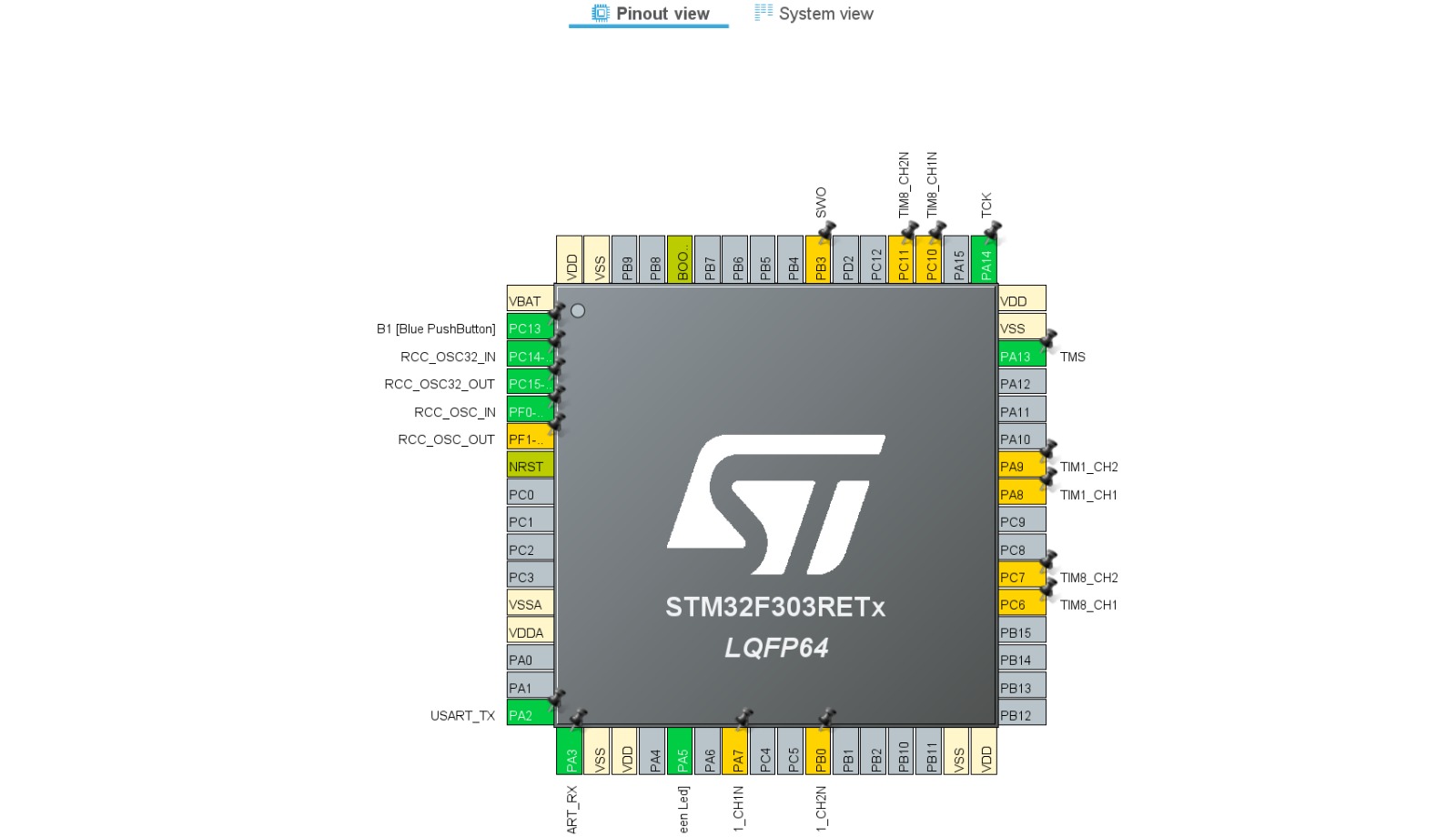
The as-wired GPIO assignments on the STM32 Nucleo-F303RE. This table supersedes the v3.1 build-guide table — see the errata at the bottom of this page.
PWM outputs (TIM1 + TIM8, complementary)¶
| Signal | Timer channel | Pin | AF |
|---|---|---|---|
| PWM_1H | TIM1_CH1 | PA8 | AF6 |
| PWM_1L | TIM1_CH1N | PA7 | AF6 |
| PWM_2H | TIM1_CH2 | PA9 | AF6 |
| PWM_2L | TIM1_CH2N | PA12 | AF6 |
| PWM_3H | TIM8_CH1 | PB6 | AF5 |
| PWM_3L | TIM8_CH1N | PB3 | AF5 |
| PWM_4H | TIM8_CH2 | PB8 | AF5 |
| PWM_4L | TIM8_CH2N | PB0 | AF5 |
Bridge 1 is driven by TIM1 (CH1/CH1N + CH2/CH2N → 4 half-bridge gate signals). Bridge 2 is driven by TIM8 (same pattern). Both timers run with BDTR.MOE, BDTR.OSSR=1, BDTR.OSSI=1 so the outputs forcibly drive LOW when MOE is off or any CCxE bit is off. Combined with the TLP250 non-inverting topology (LED ON → output HIGH → MOSFET ON), this means every MOSFET is off whenever the firmware thinks the bridge is disarmed.
Isolated sensing (bit-banged MCP3201)¶
| Signal | Pin | Notes |
|---|---|---|
| SCK | PA5 | Single shared SCK at ~140 kHz (well under MCP3201's 1.6 MHz max). |
| CS_DC1 | PC0 | Bridge 1 DC-bus ADC chip select. |
| CS_DC2 | PC1 | Bridge 2 DC-bus ADC chip select. |
| CS_CUR | PC2 | Current sensor (ACS712 → MCP3201) chip select. |
| MISO_DC1 | PA6 | Lower-bridge isolated island — DC1 ADC alone. |
| MISO_DC2 / MISO_CUR | PC3 | Upper-bridge isolated island — DC2 and current share this wire. The firmware reads strictly one channel at a time so they never collide. |
PC4 is unused — earlier firmware revisions assumed three independent MISOs; the as-built board uses two (one shared upper-island return). The firmware was rewritten to read strictly one channel per 16-clock pass, matching build-guide v3.1 §3.6.2.
UART, fault output¶
| Signal | Pin | Notes |
|---|---|---|
| USART2_TX | PA2 | ST-LINK virtual COM port. 115200 8N1. |
| USART2_RX | PA3 | Same VCP. |
| FAULT_OUT | PB5 | Active-LOW (LOW = fault latched). Drives an indicator LED or external interlock. Corresponds to build-guide v3.1 header pin 16. |
v3.1 errata (firmware is correct)¶
The official Build Guide v3.1 had two pin-assignment errors. Build Guide v4.0 carries the corrections; this page is the firmware-side reference.
| What v3.1 said | What the firmware uses | Why v3.1 is wrong |
|---|---|---|
| PWM_1L = PA10 (TIM1_CH2N) | PA12 (TIM1_CH2N AF6) | PA10 has no TIM1_CH2N alternate function on the F303RE. The valid TIM1_CH2N pins are PA12, PB0, and PB14. |
| TIM8 = PC6 / PC7 / PC8 / PC9 (CH1 / CH1N / CH2 / CH2N) | PB6 / PB3 / PB8 / PB0 (CH1 / CH1N / CH2 / CH2N AF5) | On F303RE, PC7 = TIM8_CH2 (not CH1N), PC8 = TIM8_CH3 (not CH2), PC9 = TIM8_CH4 (not CH2N). Only PC6 maps as advertised. |
Both corrections were confirmed against the actual board wiring during bring-up.