Iteration 4 — as-built (two single-bridge modules, IRFB4110, PSC)
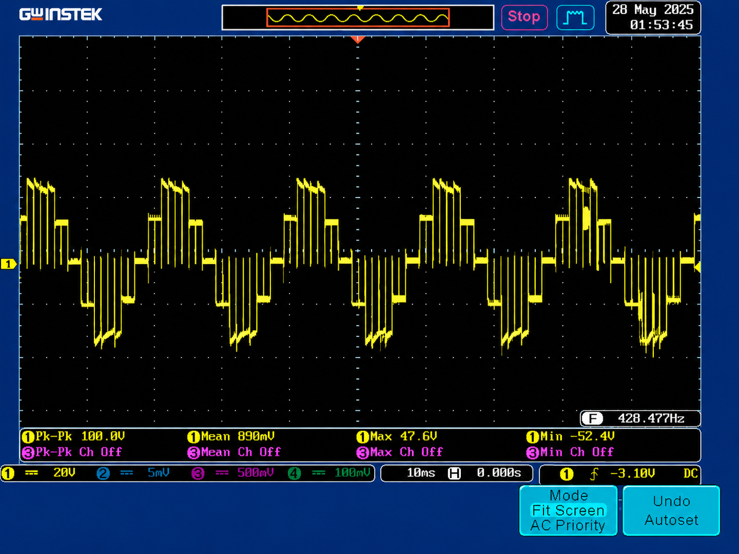
Status: as-built. Bench-validated and demonstrated. KiCad project at
hardware/single-bridge-v4/kicad/, gerbers athardware/single-bridge-v4/gerbers/, photos athardware/single-bridge-v4/photos/anddocs/assets/images/(demo day).
What was attempted
Iteration 4 was a rebuild from the iteration-3 lessons rather than a tweak on top of iteration 3. Six structural changes:
| Change | From | To | Rationale |
|---|---|---|---|
| Board topology | Single dual-bridge PCB | Two identical single-bridge PCB modules | Modularity; each cell can be bench-tested in isolation; bridges become interchangeable. |
| Stack-up | 2-layer | 4-layer, 1.6 mm FR-4, JLCPCB | Dedicated ground planes solve the 5V_GND ↔ 50V_GND coupling from iteration 3. |
| Power MOSFET | IRFZ44N (55 V) | IRFB4110 (100 V, 4.5 mΩ) | VDSS headroom; resolves the TVS clamp / MOSFET breakdown mismatch from iteration 1. |
| Modulator | IPD LS-PWM at 500 Hz | PSC-PWM at 5 kHz | Bridge-thermal symmetry; better filter behavior; better textbook THD. |
| Dead time | 2 µs (IRFZ44N) | 3 µs (BDTR.DTG = 0xA0) |
Compensates for the IRFB4110's ~2× gate charge. |
| MISO topology | 3-independent assumption | 2 MISO lines (lower-island dedicated, upper-island shared DC2 + CUR) | Reflects the actual as-fabricated routing. Firmware rewritten to sequential one-CS-at-a-time reads. |
The firmware that drives this hardware lives on the pwm-rewrite-configurable branch — imported into this repo via git subtree with full history.
What worked
The bench validation confirmed every headline goal:
| Goal | Result |
|---|---|
| 5 distinct cascade output levels visible on scope | ✅ — see the scope-pwm-cascade-output.jpeg capture in populated photos. |
| PSC carrier phase lock | ✅ — $C,...,lock=OK reported on every config line and across runs. |
| Bridges thermally matched | ✅ — within ~3 °C under sustained PSC load. |
| Sensing clean throughout the run | ✅ — no false SENSOR_LOST events, STATUS line clean over multi-minute sessions. |
| Dashboard auto-cancels firmware auto-start | ✅ — STATUS echoed on connect and on every BOOT_SELF_TEST_DONE; operator always in control when the dashboard is open. |
| Protection chain protects | ✅ — TVS clamps below MOSFET VDSS; UV/OV/OC/IMBAL with N-of-M debounce; FAULT_OUT pin pulled LOW on trip. |
What's still soft (carries over to the roadmap)
- No LC output filter. The bench demo ran into a resistive load. For non-trivial loads, the LC filter is the next item.
- Open-loop control. Modulation index is set by the operator. Closed-loop control is the natural follow-on.
- No enclosure. Open-bench operation only. See thermal enclosure.
- Bench-only verification. No compliance testing, no grid-side integration. See grid tie and product path.
What to remember about iteration 4
- It is not an incremental fix to iteration 3 — it's a re-architecture motivated by what the earlier iterations made painful.
- The modular two-PCB-module decision is the most important structural choice; everything else hangs off it (interchangeable boards, single fab order, simpler bring-up procedure).
- The IRFZ44N → IRFB4110 swap is the kind of mid-project component change that needs the firmware (dead time) and the protection chain (TVS clamp vs. MOSFET VDSS) to be updated together. Both were.
- The PSC carrier-shift lock diagnostic was added defensively before the bench session — it caught a real issue on day one and saved an afternoon of scope time.