Model architecture
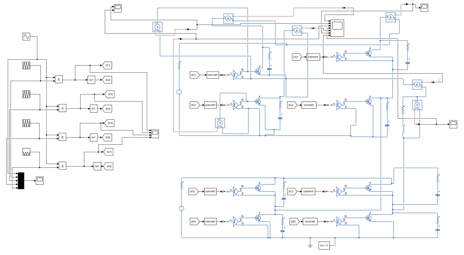
chb-5level-rl-nospike.slx) after the snubber-tuning pass that removed VDS ringing.Three Simulink models live in simulation/simulink/. They share a common block structure; the differences are in the gate-driver model, the modulator, and the load.
Common structure
flowchart LR
    Vdc1[V_DC₁] --> HB1[H-bridge 1]
    Vdc2[V_DC₂] --> HB2[H-bridge 2]
    Ref[50 Hz sine reference] --> Mod[LS-PWM / PSC
modulator]
    Mod --> HB1
    Mod --> HB2
    HB1 --> Sum[Σ cascade]
    HB2 --> Sum
    Sum -->|optional| LC[LC filter]
    LC --> Load[Resistive / RL load]
    Sum -->|no filter| Load
    Load --> Meas[Scope, FFT, THD]
Per-model details
chb-5level-v1.slx — IPD LS-PWM baseline
The first-pass model. Ideal complementary switches, no parasitics, no dead time. Used to:
- Confirm the 5-level cascade arithmetic (output level ∈ {−2, −1, 0, +1, +2}·VDC).
- Produce the headline THD = 4.9 % figure with IPD level-shifted PWM at 5 kHz.
- Validate the IEEE 519-2022 voltage-distortion compliance argument.
Inputs: two independent 50 V DC sources, 50 Hz reference, MI = 0.95. Output measurement: the cascade output is scoped + FFT'd to extract THD.
chb-5level-v2.slx — gate-driver sweep
Adds gate-driver behavioural models:
- IR2110 (bootstrap): the bootstrap capacitor follows VS of the high-side MOSFET. Because the upper bridge's VS floats at the cascade voltage, the bootstrap path never returns to true ground, and the simulated gate drive collapses to < 5 V on the upper bridge — MOSFETs fail to turn on. Output waveform: severely distorted, irrecoverable.
- TLP250 (optical): independent isolated 15 V supply per driver. All eight gates see 15 V regardless of floating potential. Output waveform: matches the ideal 5-level cascade.
This model is the evidence that killed the IR2110 path before any silicon was committed. The TLP250 → 6N137 → MCP3201 sensing chain on the actual hardware traces directly to this simulation.
chb-5level-rl-nospike.slx — RL load + LC filter sweep
Adds:
- LC output filter (parametrised — see the THD analysis for the values tried).
- RL load (10 Ω + 5 mH) to surface the wavy-current artefact under inductive load.
- No spike in the title refers to the snubber-tuning pass that removed the VDS ringing the earlier model showed.
Used to size the bench LC filter (planned roadmap item; not built).

How to run
- Install MATLAB R2023b or later with Simscape Electrical.
- Open the
.slxfile. - Press Run. Default simulation time is 100 ms (≈ 5 fundamental periods).
- The output scopes show: cascade voltage, per-bridge contributions, load current.
- To extract THD, run
thd(simout.OutputVoltage.Data, simout.OutputVoltage.Time(2) - simout.OutputVoltage.Time(1), 50).
A reusable thd-analysis.m helper is not yet committed — the team ran analysis directly in the MATLAB console. Adding the helper to simulation/matlab/ is tracked as a polish item.