Iteration 1 — single dual-bridge layout, IRFZ44N, IPD LS-PWM
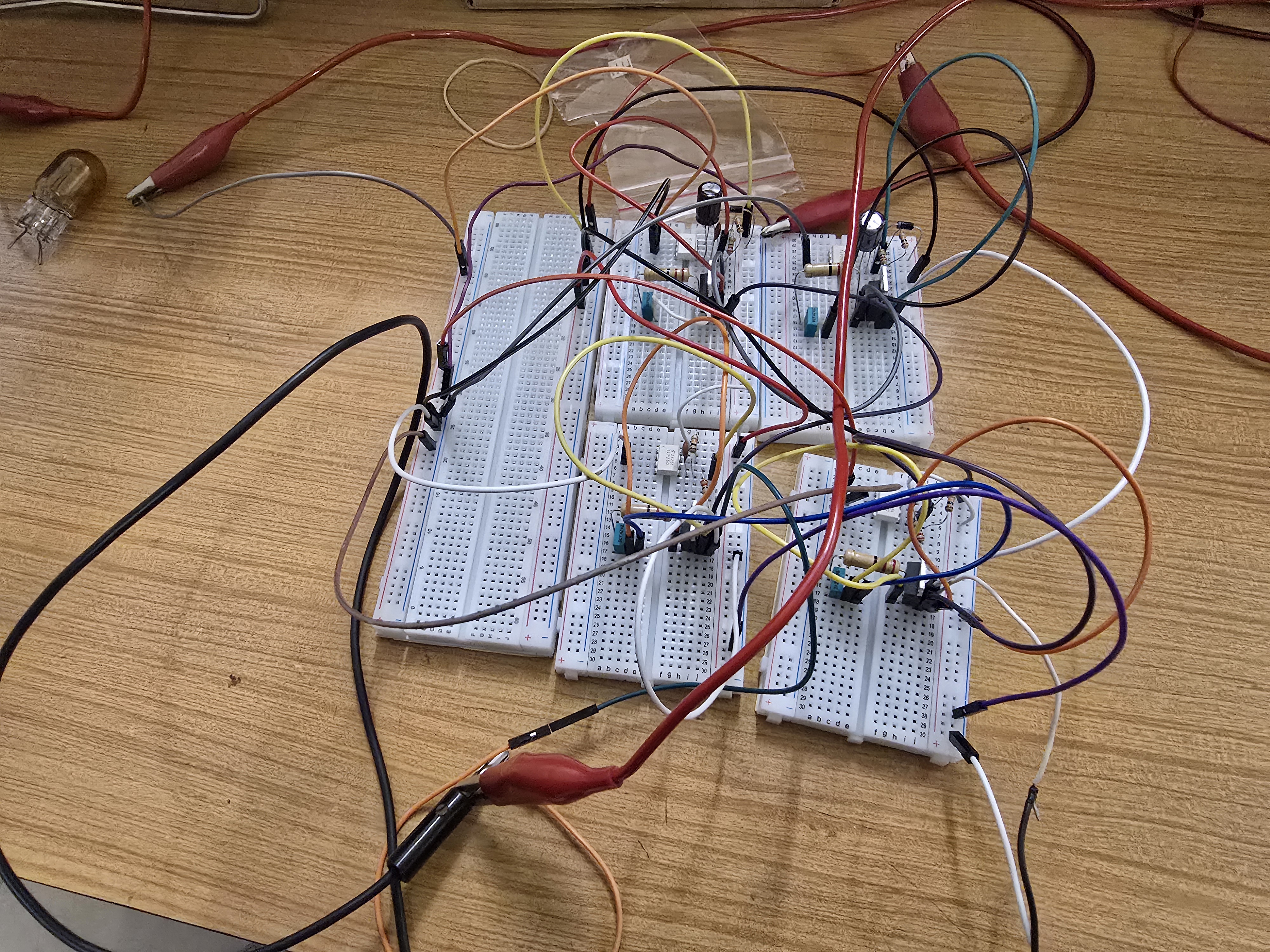
Status: superseded. Not for fabrication. KiCad files for iteration 1 are not preserved in the repo; the closest survivor is the v3.1 BOM at
hardware/legacy/iteration-3/CHB_BOM_v3_1.xlsx.
What was attempted
A single PCB that hosted both H-bridges of the 5-level cascade, with:
- 8× IRFZ44N MOSFETs (4 per bridge) in TO-220 packages, per the Build Guide v3.1 BOM.
- TLP250 optical gate drivers on every gate (this part was right from the start).
- IPD Level-Shifted Carrier PWM at 500 Hz, generated by the STM32 Nucleo-F303RE.
- Three independent MCP3201 ADCs (DC1, DC2, current), each with its own MISO line back to the controller (the firmware's original "3-MISO" assumption).
The intent was the simplest-possible 5-level inverter — one board, one bring-up, and the most-textbook modulation strategy.
What failed
| Failure | What happened | Why |
|---|---|---|
| MOSFET VDSS too tight | IRFZ44N VDSS = 55 V; bench supplies at 50 V plus switching spikes brought peak VDS uncomfortably close to breakdown. | At a 50 V bus the headroom is barely 10 % nominal; spikes from gate-loop parasitics ate that margin. |
| TVS / VDSS mismatch | 1.5KE62A TVS clamps at 84.5 V — above IRFZ44N VDSS. A TVS firing event would still damage the MOSFETs. | Latent BOM hazard. The TVS was sized for a higher-VDSS MOSFET than what was specified. |
| Bridge-1 thermal asymmetry | With IPD LS-PWM, Bridge 1 always carried the inner-band switching (±1 step). One of Bridge 1's MOSFETs ran measurably warmer than its counterparts. | The IPD mapping puts the most-switched bridge in a fixed role for the whole fundamental period. See PSC vs. LSPWM. |
| 3-MISO firmware assumption | The firmware read three MCP3201 MISO lines in parallel during the SPI scan, assuming each ADC had its own dedicated return. | This worked on the iteration-1 layout — the issue surfaced later when the modular per-bridge isolation made the MISO scheme harder to maintain. |
What was learned
- Voltage headroom is not optional. A 10 % margin above nominal bus isn't enough when gate-loop parasitics add tens of volts of ringing. Iteration 4 raised VDSS headroom to ≈ 2×.
- The protection chain has to actually protect. If the TVS clamps above the MOSFET VDSS, a TVS event is still a MOSFET kill. Check the clamp voltage against the MOSFET rating before ordering.
- Modulator choice has thermal consequences. Symmetric (PSC) vs. asymmetric (IPD) modulation directly translates to whether the bridges run at the same temperature. This wasn't obvious at design time; the bench measurements made it concrete.
What changed for iteration 2
- Schematic split into modular sheets (the start of the
Highside_cell/Lowside_cell/driver_celldecomposition that survives in the iteration-4 KiCad). - Gate-drive routing redrawn around bootstrap timing concerns — leading directly into the bootstrap fundamentals discussion in iteration 2.
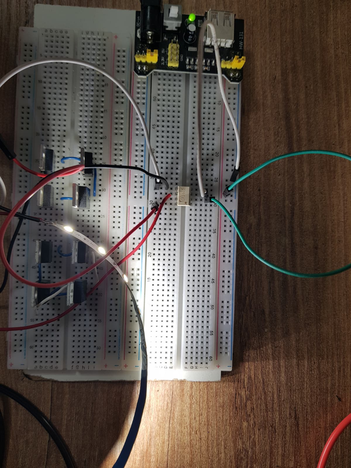
The IRFZ44N and the IPD LS-PWM choice were both kept, on the theory that they were "good enough" and the layout was the bigger risk. Both assumptions were reversed by iteration 4.